Nintendo Switch 2 suppliers and component map
Who makes the Nintendo Switch 2 chip, RAM and storage? Eighteen source-linked records separate Nintendo's specifications, iFixit and TechInsights teardown findings, a reported Samsung 8N-class die analysis and Bloomberg-reported assemblers.
- 供应商
- 15
- 部件记录
- 18
- 分类
- 6
- 来源
- 9
- 发布年份
- 2025
- 最近审核
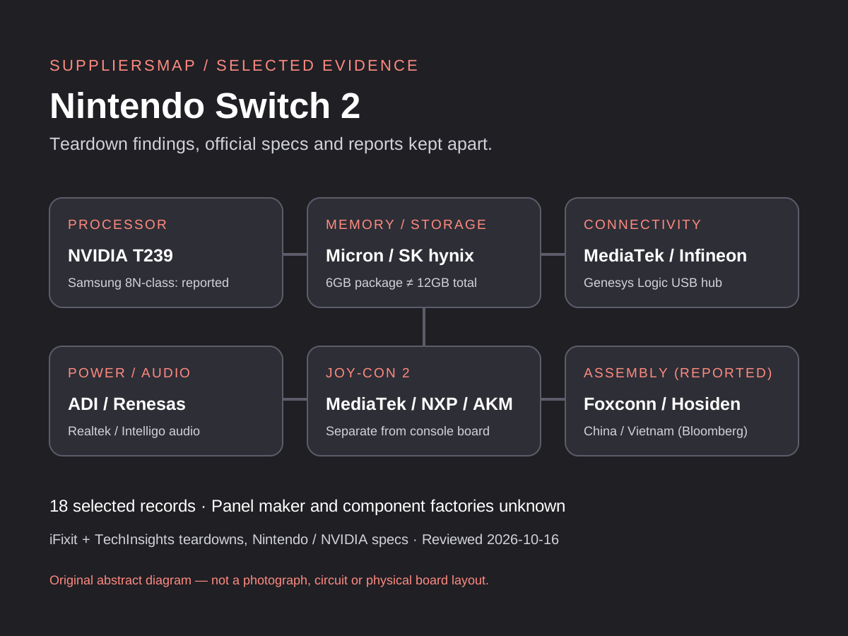
Nintendo Switch 2 关键芯片与供应商
6 个分类一览,点卡片跳到对应记录。
- Processor2 条记录NVIDIA, Samsung FoundryCustom SoC — GMLX30-A1 (T239)官方规格拆解确认媒体报道
- Memory and storage3 条记录Micron, SK hynix6GB memory package — MT62F768M64D4EK-026拆解确认媒体报道
- Connectivity and USB3 条记录MediaTek, Infineon, Genesys LogicWi-Fi / Bluetooth — MT3681AEN拆解确认
- Power and audio5 条记录Analog Devices, Renesas, Realtek, Intelligo TechnologyPower management — MAX77851拆解确认
- Joy-Con 2 controllers3 条记录MediaTek, NXP Semiconductors, AKM SemiconductorBluetooth SoC — MT3689BCA拆解确认
- Final assembly (reported)2 条记录Foxconn, HosidenConsole assembly — mainly China (reported)媒体报道
Nintendo Switch 2 全部 18 条供应商记录
按分类分组。每条记录都链接到来源;位置为空表示未知。
- 官方规格厂商披露或官方规格
- 拆解确认由拆解或芯片分析机构第一手确认
- 媒体报道媒体报道或媒体转述的机构结论,尚未确认
Processor
· 2 条记录NVIDIA
Custom SoC — GMLX30-A1 (T239)
- 作用
- Custom processor (CPU + GPU)
- 范围
- All units per Nintendo; package marking from iFixit's board
- 证据记录
- NVIDIA — GMLX30-A1 (T239)
位置: 未知
官方规格拆解确认证据: Nintendo / NVIDIA disclosure; iFixit identification
Samsung Foundry
SoC fabrication — 8N-class (reported)
- 作用
- SoC fabrication
- 范围
- Engineering-board die analysis; not officially confirmed
- 证据记录
- Samsung Foundry — 8N-class process
位置: 未知
媒体报道证据: Reported (Tom's Hardware on Geekerwan analysis)
Memory and storage
· 3 条记录Micron
6GB memory package — MT62F768M64D4EK-026
- 作用
- 6GB memory package
- 范围
- iFixit board; one package, not the system total
- 证据记录
- Micron — MT62F768M64D4EK-026 WT:B
位置: 未知
拆解确认证据: iFixit identification
SK hynix
2 × 6GB LPDDR5X (12GB total)
- 作用
- Main memory, 12GB total
- 范围
- TechInsights unit; also reported on the engineering board
- 证据记录
- SK hynix — 6GB LPDDR5X × 2
位置: 未知
媒体报道证据: TechInsights teardown
SK hynix
256GB UFS 3.1 — HN8T15DEHKX075
- 作用
- 256GB NAND with UFS 3.1 controller
- 范围
- Part number from iFixit's board; TechInsights lists SK hynix 256GB UFS 3.1 without the part number
- 证据记录
- SK hynix — HN8T15DEHKX075
位置: 未知
拆解确认证据: iFixit part ID; vendor role also in TechInsights
Connectivity and USB
· 3 条记录MediaTek
Wi-Fi / Bluetooth — MT3681AEN
- 作用
- Wi-Fi and Bluetooth controller
- 范围
- Console main board
- 证据记录
- MediaTek — MT3681AEN
位置: 未知
拆解确认证据: iFixit part ID; vendor role also in TechInsights
Infineon
USB Type-C controller — CP10359AT
- 作用
- USB Type-C controller
- 范围
- Console main board
- 证据记录
- Infineon — CP10359AT
位置: 未知
拆解确认证据: iFixit part ID; vendor role also in TechInsights
Genesys Logic
USB 2.0 hub — GL852G
- 作用
- USB 2.0 hub
- 范围
- Console main board
- 证据记录
- Genesys Logic — GL852G
位置: 未知
拆解确认证据: iFixit part ID; vendor role also in TechInsights
Power and audio
· 5 条记录Analog Devices
Power management — MAX77851
- 作用
- Power management IC
- 范围
- Console main board
- 证据记录
- Analog Devices — MAX77851
位置: 未知
拆解确认证据: iFixit identification
Analog Devices
Battery charger — MAX77986
- 作用
- Single-cell Li-ion battery charger
- 范围
- Console main board
- 证据记录
- Analog Devices — MAX77986
位置: 未知
拆解确认证据: iFixit identification
Renesas
Power management — DA9092
- 作用
- Power management IC
- 范围
- Console main board
- 证据记录
- Renesas — DA9092
位置: 未知
拆解确认证据: iFixit part ID; vendor role also in TechInsights
Realtek
Audio codec — ALC5658
- 作用
- Audio codec
- 范围
- Console main board
- 证据记录
- Realtek — ALC5658
位置: 未知
拆解确认证据: iFixit identification
Intelligo Technology
Voice processor — IG2200
- 作用
- Audio / voice processor
- 范围
- Console main board
- 证据记录
- Intelligo Technology — IG2200
位置: 未知
拆解确认证据: iFixit identification
Joy-Con 2 controllers
· 3 条记录MediaTek
Bluetooth SoC — MT3689BCA
- 作用
- Bluetooth SoC
- 范围
- Joy-Con 2 board, not the console
- 证据记录
- MediaTek — MT3689BCA
位置: 未知
拆解确认证据: iFixit part ID; vendor role also in TechInsights
NXP Semiconductors
NFC controller — PN7160
- 作用
- NFC controller
- 范围
- Joy-Con 2 board
- 证据记录
- NXP Semiconductors — PN7160
位置: 未知
拆解确认证据: iFixit identification
AKM Semiconductor
3-axis compass — AK09919C
- 作用
- 3-axis electronic compass
- 范围
- Joy-Con 2 board
- 证据记录
- AKM Semiconductor — AK09919C
位置: 未知
拆解确认证据: iFixit part ID; vendor role also in TechInsights
Final assembly (reported)
· 2 条记录Foxconn
Console assembly — mainly China (reported)
- 作用
- Console final assembly
- 范围
- Console made mainly in China by partners including Foxconn; plant unstated
- 证据记录
- Foxconn
位置: China
媒体报道证据: Reported (Bloomberg)
Hosiden
Console assembly — Vietnam exports (reported)
- 作用
- Console final assembly
- 范围
- One of three main assemblers; US shipments from Vietnam
- 证据记录
- Hosiden
位置: Vietnam
媒体报道证据: Reported (Bloomberg, customs data)
Each colored rectangle and flow counts one selected record, not cost, market share or chip quantity. Rows marked reported rely on die analysis or news reporting rather than a first-hand board identification. Blank locations mean Unknown; only the two Bloomberg-reported assembly countries are located.
Nintendo Switch 2: chip, RAM, storage and assembly evidence
Sources reviewed:
This independently written selection combines Nintendo's official Switch 2 specifications (a custom processor made by NVIDIA, a 7.9-inch 1920x1080 LCD and 256GB of UFS storage) with component identifications from iFixit's June 10, 2025 chip-ID guide and TechInsights' teardown summary published January 23, 2026. Neither teardown states the unit's sales region or production batch. A Samsung 8N-class process for the T239 comes from independent die analysis of an engineering board reported by Tom's Hardware; Nintendo and NVIDIA have not confirmed the foundry. Final-assembly rows are Bloomberg reports based on industry sources and customs data, not Nintendo disclosures.
NVIDIA designs the chip; the foundry is a reported finding
Nintendo's specifications say the CPU/GPU is a custom processor made by NVIDIA, and NVIDIA describes a custom processor with RT Cores and Tensor Cores. iFixit reads the package as NVIDIA GMLX30-A1. Independent die analysis of an engineering board, reported by Tom's Hardware, found the T239 codename on the die and a customized Samsung 8N-class process. That last point is reported, not officially confirmed.
12GB of RAM, 6GB packages and more than one memory vendor
TechInsights lists two 6GB LPDDR5X packages from SK hynix, 12GB in total. iFixit's chip-ID guide identifies a Micron 6GB package on its board instead. Both can be true for different units: consoles are often multi-sourced. The map keeps both records, scoped to their samples, rather than naming one universal memory supplier.
Who builds the console is separate from who makes its chips
Nintendo does not name its assemblers. Bloomberg reports that the Switch 2 is manufactured mainly in China by partners including Foxconn, and that Hosiden, one of three main assemblers, shipped consoles to the US from Vietnam. These are assembly relationships; they do not locate where the NVIDIA, memory or storage chips themselves are made.
Limitations (6)
- Sample boundary: physical part numbers describe the boards those sources examined. Memory differs between samples (Micron in iFixit's guide; SK hynix in TechInsights' teardown and the engineering board), so neither vendor is an exclusive or universal Switch 2 memory supplier. Later revisions may differ.
- 6GB is the capacity of one memory package. TechInsights lists two 6GB SK hynix packages (12GB total); Nintendo's own specifications do not state system RAM. iFixit's guide labels the Micron package LPDDR5; TechInsights and Tom's Hardware describe the memory as LPDDR5X.
- The display panel maker is not assigned. Nintendo specifies a 7.9-inch 1920x1080 LCD but names no panel vendor. Nikkei reported in August 2024 that Sharp aimed to supply LCDs for game consoles, without a confirmed Switch 2 attribution; Innolux and Sharp panel attributions circulate only in community wikis, reseller listings and blogs, so both are omitted.
- The Samsung foundry row is a reported die-analysis finding (Geekerwan, via Tom's Hardware) on an engineering board, described as a customized Samsung 10nm/8nm-class process. It is not an official Nintendo or NVIDIA statement. The T239 codename also comes from that die analysis; iFixit reads the package marking as GMLX30-A1.
- Foxconn and Hosiden rows are Bloomberg reporting. Bloomberg says the console is made mainly in China by partners including Foxconn, and that Hosiden, one of three main assemblers, ships from Vietnam. The third main assembler, specific plants and production shares are not established here.
- Where iFixit and TechInsights are both cited, part numbers come from iFixit's guide; TechInsights' public summary confirms the vendor and role but not the part number. Samsung memory and Kioxia storage variants, the battery cell, backlight, dock components and tentative iFixit labels (B2423 game-card controller, MAX18000 converter) are omitted. iFixit's teardown article separately mentions Micron storage modules, which conflicts with its chip-ID guide's SK hynix UFS identification, so that article sentence is not used. This is not a complete bill of materials; the evidence section is written in English.
Sources
- Nintendo: Switch 2 technical specifications — Accessed 2026-10-16; publication date not stated
- Nintendo: Switch 2 release announcement and specifications — 2025-04-02
- NVIDIA: custom processor in Nintendo Switch 2 — 2025-04-03
- iFixit: Nintendo Switch 2 Chip ID — first-hand board identification — 2025-06-10
- TechInsights teardown summary (Electronics360) — 2026-01-23
- Tom's Hardware: T239 die analysis — Samsung 8N-class process (reported) — 2025-05-07
- Bloomberg via The Japan Times: made mainly in China by partners including Foxconn — 2025-06-11
- Bloomberg: Hosiden, one of three main Switch 2 assemblers, ships from Vietnam — 2025-04-10
- The Verge: quotes Bloomberg's Hosiden customs-data report — 2025-04-10
Each colored rectangle and flow counts one selected record, not cost, market share or chip quantity. Rows marked reported rely on die analysis or news reporting rather than a first-hand board identification. Blank locations mean Unknown; only the two Bloomberg-reported assembly countries are located.
Selected component / organization records • No procurement-volume or market-share data
Nintendo Switch 2 — selected reported parts and assemblers
iFixit / TechInsights samples; region / batch unstated | Reviewed 2026-10-16 | Component factories unknown
Nintendo Switch 2 供应商常见问题
关于这条供应链的 7 个问题,答案依据上方的记录。
What chip does the Nintendo Switch 2 use?
Nintendo specifies a custom processor made by NVIDIA, and NVIDIA describes a custom chip with RT Cores and Tensor Cores (sources [1] and [3]). iFixit reads the package marking as NVIDIA GMLX30-A1 (source [4]); independent die analysis found the T239 codename on the die (source [6]).
Is the Switch 2 chip made by Samsung on 8nm?
Reportedly. Die analysis of an engineering board, reported by Tom's Hardware, found a customized Samsung 10nm/8nm-class process similar to NVIDIA's 8N (source [6]). Nintendo and NVIDIA have not confirmed the foundry, so this page labels it reported.
How much RAM does the Switch 2 have, and who makes it?
TechInsights lists two 6GB SK hynix LPDDR5X packages, 12GB in total (source [5]). iFixit's chip-ID guide shows a Micron 6GB package on its board (source [4]). Memory appears to be multi-sourced; Nintendo's specifications do not list system RAM.
Who makes the Switch 2 storage?
Nintendo specifies 256GB of UFS storage (source [1]). Both iFixit and TechInsights identify an SK hynix 256GB NAND package with a UFS 3.1 controller, HN8T15DEHKX075 in iFixit's guide (sources [4] and [5]). Other vendors in other units are not ruled out.
Who makes the Switch 2 screen?
Unknown in this map. Nintendo specifies a 7.9-inch 1920x1080 wide-color-gamut LCD with HDR10 and VRR up to 120Hz, but names no panel maker. Sharp and Innolux attributions have not been confirmed by a teardown or major outlet we could verify, so they are omitted.
Where is the Nintendo Switch 2 assembled?
Bloomberg reports the console is made mainly in China by partners including Foxconn (source [7]), and that Hosiden, one of three main assemblers, ships consoles to the US from Vietnam (sources [8] and [9]). Nintendo does not disclose its assemblers or plants.
Does this cover the Joy-Con 2 controllers and every Switch 2 revision?
Joy-Con 2 parts are listed separately from console parts (source [4]). Teardown findings cover the units examined at the time; sales region and batch are unstated, and later revisions, the dock, battery and display supply chains need separate evidence.

关于 Nintendo
Nintendo Switch 2 由 Nintendo 设计;本图列出其背后的供应商。
- 成立
- 1889
- 总部
- Kyoto, Japan
- 行业
- Video game hardware and software
- SuppliersMap 收录
- 1 款产品
相关供应链图谱
将 Nintendo Switch 2 与同一公司、同一行业的其他产品对比。